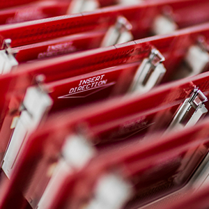
Singlelayer and Multilayer PCB
There are several different superstructures for circuit boards. The rigid area of circuit boards is divided into all kinds of superstructures made of standard FR4 materials with 35µm copper plating and soldering mask paint with ident print, special structures with aluminium layers for a better temperature distribution, higher copper structures of up to 105 µm, areas drilled by laser, special milled surfaces in Z-axis and various designs of the surface (tin/silver, HAL lead free, gold etc.).
To meet the requirements of the packing density for modern SMD components, especially those operated in computers, it is not sufficient if the conducting paths are located only on one side of the printed circuit boards. It must be ensured that all components on a circuit board are supplied with power.
After double sided circuit boards with a copper layer on both sides have been designed several thin circuit boards were stuck to each other with what is called “pre-pegs”. The multi layer circuit boards may be composed of up to 48 layers.o 48 layers.


